U.FL (IPEX/MHF) on your PCB: layout tips and gotchas for reliable RF performance
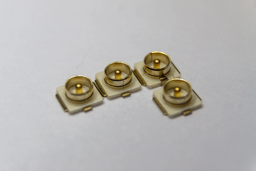
Here's a scenario that plays out weekly in some lab somewhere: a board comes back from fab, populated, powered up, and the RF link is garbage. Range is half what it should be. Someone spends three days chasing firmware bugs before anyone even looks at the connector footprint. Turns out the ground stitching was an afterthought. That tiny U.FL jack, barely bigger than a grain of rice, had been treated like any other component drop instead of the RF-critical part it actually is. This piece is our attempt to save you those three days.
What U.FL actually is, in plain terms
U.FL is Hirose's trademark, though in the wild you'll hear it called IPEX or MHF depending on who assembled your cable and which decade they learned the trade in. Same rough idea across all three: a miniature coaxial connector soldered straight onto the board, mated with a matching plug on a thin coax pigtail. You'll find these wherever board space is tight and an external antenna needs a wire back to the radio - WiFi modules, cellular modems, GPS pucks, the works. Frequency ceiling depends entirely on which variant you're using, so don't assume; pull the actual Hirose datasheet for your part number before you commit to a design running above a few GHz.
How it behaves mechanically, and why that matters before you even think about RF
This connector is small and it is not tough. Mate it a couple dozen times and you're pushing your luck - Hirose rates most variants for something like 30 mating cycles, not the thousands you'd expect from a chunky SMA. The plug seats with a straight-down push and a firm little click, and that insertion force, modest as it sounds, transmits right into your PCB. Flex the board while mating and you risk lifting pads or cracking the ceramic.
Plan your assembly process (and your end users, if they'll ever touch this thing) around gentle, infrequent mating. If your product involves techs swapping antennas daily, U.FL is the wrong choice entirely - look at something board-mounted and beefier.
Getting the footprint and land pattern right
Start from Hirose's own recommended pad geometry. Don't eyeball it, don't "improve" it based on vibes - these dimensions were worked out for a reason, and deviating tends to bite you later in ways that are hard to trace back to the footprint. You've got a center signal pad and a ring or set of ground pads surrounding it, and the spacing between them is part of what keeps the impedance sane right at the connector transition.
Solder mask treatment matters more than people expect. Some variants want solder-mask-defined pads, others want the mask pulled back further than you'd instinctively draw it. Get this wrong and you'll see solder wicking under the connector body or, worse, tombstoning during reflow where the tiny part just tips itself sideways like a felled tree. Also - and this trips people up constantly - keep any trace entering the signal pad short, straight, and centered. Don't route across the pad at an angle just because it's convenient for your layout. It isn't worth the mismatch.
Stencil design deserves its own five minutes of thought too. Reduce paste volume slightly compared to what a generic calculation gives you; too much paste under a part this light and it'll float or tombstone the moment reflow hits its peak.
Routing the RF trace without wrecking your impedance
Shortest possible path, always. Every millimeter between the connector and your first RF component - filter, matching network, front-end module, whatever - is a millimeter where things can go sideways electrically. At 2.4 GHz that's forgiving. At 5 GHz or above, it stops being forgiving fast.
Pick a controlled-impedance structure for the trace - microstrip if you've got a solid ground layer right underneath, coplanar waveguide with ground if your stackup or space constraints favor it. CPW tends to be the better call in cramped layouts since the flanking ground pours help contain the field and cut down on stray radiation. Whichever you choose, run the numbers through an impedance calculator against your actual stackup - don't just copy a trace width from some other design with different dielectric thickness.
Vias in the signal path are trouble. A single via, modeled properly, is tolerable if you absolutely must jump layers - but treat every additional via as a small tax on your return loss. Avoid abrupt width steps, sharp bends, or little stub traces hanging off the main line near the connector; these read as discontinuities at RF even though they'd be invisible at DC.
Grounding and stitching - where most boards actually fail
Here's the part that gets skipped most often, and it's the part that costs people the most. Stitch ground vias tightly around the connector body itself. This gives your return current a genuinely low-inductance path back rather than forcing it to hunt for the nearest via three centimeters away. Place small ground vias right up against the ground pads in the footprint, and make sure they actually land on your internal ground plane rather than floating on an isolated pour.
Don't let a power-plane split or an analog/digital ground boundary wander underneath the connector. If the return path has to detour around a gap in copper, you've built yourself a discontinuity, and it'll show up as an ugly bump in your S11 sweep. For CPW structures specifically, keep the ground pour symmetric on both sides and stitch vias every millimeter or two depending on frequency - loosen that spacing and you risk parasitic resonances sneaking into your passband.
Where to put it and what to leave clear around it
Corner or edge placement usually wins for ease of mating and cable routing, though it does put more mechanical stress on that corner of the board during handling. Keep tall components away from the immediate vicinity - you need clearance not just for the plug itself but for whatever tool you or your assembly line uses to seat and remove it. Think about which direction the cable will exit and avoid forcing a tight bend right at the plug; a strain relief, even something as basic as a dab of hot glue or a chassis clamp, saves you from fatigue failures down the line. If your board carries more than one U.FL connector, standardize their orientation. Future-you, doing harness assembly at 11pm before a demo, will thank present-you.
Reflow and assembly quirks worth knowing
Follow the vendor's reflow profile, not a generic one borrowed from another BOM line. Pick-and-place accuracy matters more here than for most passives given how small the footprint tolerances are. After reflow, actually inspect the seating - a connector that's sitting slightly proud or slightly sunk can prevent the mating plug from clicking home fully, and you might not notice until someone's fighting with a cable on the bench. For designs facing vibration, some engineers add a dab of epoxy for mechanical backup, but confirm first that it doesn't creep under the connector body and mess with the dielectric.
Gotchas that show up again and again
Mirrored footprints are shockingly common - someone flips the part in the library and nobody catches it until the plug physically won't seat right. Ground stitching gaps show up later as return loss spikes that look mysterious until you finally pull up the layout. Bad stencil design gives you tombstoned or lifted connectors with intermittent contact that only fails intermittently, which is the worst kind of bug to chase. And rough mating over time can bend or snap the tiny center pin - if a previously working link suddenly goes deaf, pull the cable and actually look at the contact under magnification before assuming it's a firmware bug.
Proving it works before you commit to a production run
Get a network analyzer on it. Measure S11 with a known-good pigtail and a short reference cable so you're characterizing the connector transition, not your test setup. Run some mechanical mating cycles to make sure the connector survives what your assembly process will throw at it, and if vibration is part of the product's life, test for that too. X-ray inspection is worth it if you suspect a reflow issue you can't see from the top. And honestly, just build a handful of prototype boards before you commit to a full run - the cost of catching a bad footprint at prototype stage is nothing compared to catching it after a few thousand units are in a warehouse.
The short version, if you're skimming
Grab the vendor's footprint and don't modify the pad geometry. Route the shortest possible 50-ohm trace and keep vias out of the signal path if you can help it. Stitch ground vias densely around the connector body. Leave room to actually mate the thing and support the cable mechanically. Build a prototype and check S11 before you order the full run.
The bottom line, such as it is
U.FL rewards careful layout and punishes sloppy shortcuts almost immediately. Stick close to the vendor's guidance, respect the impedance math, and give it a prototype run before you trust it with production.